- 您现在的位置:买卖IC网 > Sheet目录312 > AT25DF321-SU (Atmel)IC FLASH 32MBIT 70MHZ 8SOIC
�� �
�
�AT25DF321�
�9.2�
�Write� Disable�
�The� Write� Disable� command� is� used� to� reset� the� Write� Enable� Latch� (WEL)� bit� in� the� Status� Reg-�
�ister� to� the� logical� “0”� state.� With� the� WEL� bit� reset,� all� program,� erase,� Protect� Sector,� Unprotect�
�Sector,� and� Write� Status� Register� commands� will� not� be� executed.� The� Write� Disable� command�
�is� also� used� to� exit� the� Sequential� Program� Mode.� Other� conditions� can� also� cause� the� WEL� bit�
�to� be� reset;� for� more� details,� refer� to� the� WEL� bit� section� of� the� Status� Register� description� on�
�page� 21� .�
�To� issue� the� Write� Disable� command,� the� CS� pin� must� first� be� asserted� and� the� opcode� of� 04h�
�must� be� clocked� into� the� device.� No� address� bytes� need� to� be� clocked� into� the� device,� and� any�
�data� clocked� in� after� the� opcode� will� be� ignored.� When� the� CS� pin� is� deasserted,� the� WEL� bit� in�
�the� Status� Register� will� be� reset� to� a� logical� “0”.� The� complete� opcode� must� be� clocked� into� the�
�device� before� the� CS� pin� is� deasserted,� and� the� CS� pin� must� be� deasserted� on� an� even� byte�
�boundary� (multiples� of� eight� bits);� otherwise,� the� device� will� abort� the� operation� and� the� state� of�
�the� WEL� bit� will� not� change.�
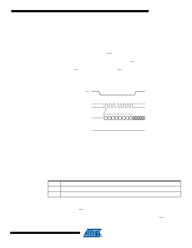
�Figure� 9-2.�
�Write� Disable�
�CS�
�0�
�1�
�2�
�3�
�4�
�5�
�6�
�7�
�SCK�
�OPCODE�
�SI�
�0�
�0�
�0�
�0�
�0�
�1�
�0�
�0�
�MSB�
�SO�
�HIGH-IMPEDANCE�
�9.3�
�Protect� Sector�
�Every� physical� sector� of� the� device� has� a� corresponding� single-bit� Sector� Protection� Register�
�that� is� used� to� control� the� software� protection� of� a� sector.� Upon� device� power-up� or� after� a�
�device� reset,� each� Sector� Protection� Register� will� default� to� the� logical� “1”� state� indicating� that� all�
�sectors� are� protected� and� cannot� be� programmed� or� erased.�
�Issuing� the� Protect� Sector� command� to� a� particular� sector� address� will� set� the� corresponding�
�Sector� Protection� Register� to� the� logical� “1”� state.� The� following� table� outlines� the� two� states� of�
�the� Sector� Protection� Registers.�
�Table� 9-1.�
�Value�
�0�
�1�
�Sector� Protection� Register� Values�
�Sector� Protection� Status�
�Sector� is� unprotected� and� can� be� programmed� and� erased.�
�Sector� is� protected� and� cannot� be� programmed� or� erased.� This� is� the� default� state.�
�Before� the� Protect� Sector� command� can� be� issued,� the� Write� Enable� command� must� have� been�
�previously� issued� to� set� the� WEL� bit� in� the� Status� Register� to� a� logical� “1”.� To� issue� the� Protect�
�Sector� command,� the� CS� pin� must� first� be� asserted� and� the� opcode� of� 36h� must� be� clocked� into�
�the� device� followed� by� three� address� bytes� designating� any� address� within� the� sector� to� be�
�locked.� Any� additional� data� clocked� into� the� device� will� be� ignored.� When� the� CS� pin� is� deas-�
�serted,� the� Sector� Protection� Register� corresponding� to� the� physical� sector� addressed� by� A23-�
�13�
�3669B–DFLASH–6/09�
�发布紧急采购,3分钟左右您将得到回复。
相关PDF资料
AT25F1024AN-10SU-2.7
IC FLASH 1MBIT 33MHZ 8SOIC
AT25F2048N-10SU-2.7
IC FLASH 2MBIT 33MHZ 8SOIC
AT25F4096W-10SU-2.7
IC FLASH 4MBIT 33MHZ 8SOIC
AT25HP512W2-10SI-2.7 SL383
IC EEPROM 512KBIT 10MHZ 16SOIC
AT26DF081A-SSU
IC FLASH 8MBIT 70MHZ 8SOIC
AT26DF161-SU
IC FLASH 16MBIT 66MHZ 8SOIC
AT26DF161A-MU
IC FLASH 16MBIT 70MHZ 8QFN
AT26DF321-SU
IC FLASH 32MBIT 66MHZ 8SOIC
相关代理商/技术参数
AT25DF512C-MAHNGU-T
功能描述:IC FLASH 512KB 8UDFN 制造商:adesto technologies 系列:- 包装:带卷(TR) 零件状态:有效 格式 - 存储器:闪存 存储器类型:FLASH 存储容量:512K(64K x 8) 速度:85MHz 接口:SPI 串行 电压 - 电源:1.65 V ~ 3.6 V 工作温度:-40°C ~ 85°C(TC) 封装/外壳:8-UFDFN 裸露焊盘 供应商器件封装:8-UDFN(2x3) 标准包装:5,000
AT25DF512C-MAHNGU-Y
功能描述:IC FLASH 512KB 8UDFN 制造商:adesto technologies 系列:- 包装:托盘 零件状态:停产 格式 - 存储器:闪存 存储器类型:FLASH 存储容量:512K(64K x 8) 速度:85MHz 接口:SPI 串行 电压 - 电源:1.65 V ~ 3.6 V 工作温度:-40°C ~ 85°C(TC) 封装/外壳:8-UFDFN 裸露焊盘 供应商器件封装:8-UDFN(2x3) 标准包装:490
AT25DF512C-MAHN-T
功能描述:IC FLASH 512KB 8UDFN 制造商:adesto technologies 系列:- 包装:剪切带(CT) 零件状态:有效 格式 - 存储器:闪存 存储器类型:FLASH 存储容量:512K(64K x 8) 速度:85MHz 接口:SPI 串行 电压 - 电源:1.65 V ~ 3.6 V 工作温度:-40°C ~ 85°C(TC) 封装/外壳:8-UFDFN 裸露焊盘 供应商器件封装:8-UDFN(2x3) 标准包装:1
AT25DF512C-MAHN-Y
功能描述:IC FLASH 512KB 8UDFN 制造商:adesto technologies 系列:- 包装:托盘 零件状态:停产 格式 - 存储器:闪存 存储器类型:FLASH 存储容量:512K(64K x 8) 速度:85MHz 接口:SPI 串行 电压 - 电源:1.65 V ~ 3.6 V 工作温度:-40°C ~ 85°C(TC) 封装/外壳:8-UFDFN 裸露焊盘 供应商器件封装:8-UDFN(2x3) 标准包装:490
AT25DF512C-SSHN-B
功能描述:IC FLASH 512KB 8SOIC 制造商:adesto technologies 系列:- 包装:管件 零件状态:有效 格式 - 存储器:闪存 存储器类型:FLASH 存储容量:512K(64K x 8) 速度:85MHz 接口:SPI 串行 电压 - 电源:1.65 V ~ 3.6 V 工作温度:-40°C ~ 85°C(TC) 封装/外壳:8-SOIC(0.154",3.90mm 宽) 供应商器件封装:8-SOIC 标准包装:98
AT25DF512C-SSHNGU-B
功能描述:IC FLASH 512KB 8SOIC 制造商:adesto technologies 系列:- 包装:管件 零件状态:有效 格式 - 存储器:闪存 存储器类型:FLASH 存储容量:512K(64K x 8) 速度:85MHz 接口:SPI 串行 电压 - 电源:1.65 V ~ 3.6 V 工作温度:-40°C ~ 85°C(TC) 封装/外壳:8-SOIC(0.154",3.90mm 宽) 供应商器件封装:8-SOIC 标准包装:98
AT25DF512C-SSHNGU-T
功能描述:IC FLASH 512KB 8SOIC 制造商:adesto technologies 系列:- 包装:带卷(TR) 零件状态:有效 格式 - 存储器:闪存 存储器类型:FLASH 存储容量:512K(64K x 8) 速度:85MHz 接口:SPI 串行 电压 - 电源:1.65 V ~ 3.6 V 工作温度:-40°C ~ 85°C(TC) 封装/外壳:8-SOIC(0.154",3.90mm 宽) 供应商器件封装:8-SOIC 标准包装:4,000
AT25DF512C-SSHN-T
功能描述:IC FLASH 512KB 8SOIC 制造商:adesto technologies 系列:- 包装:剪切带(CT) 零件状态:停产 格式 - 存储器:闪存 存储器类型:FLASH 存储容量:512K(64K x 8) 速度:85MHz 接口:SPI 串行 电压 - 电源:1.65 V ~ 3.6 V 工作温度:-40°C ~ 85°C(TC) 封装/外壳:8-SOIC(0.154",3.90mm 宽) 供应商器件封装:8-SOIC 标准包装:1